

India Notifies Semicon 2.0 Scheme Worth 1.27 Lakh Crore Rupees Covering Design, Fabs And Packaging
The government has formally opened its next chapter of chip ambitions, widening eligibility to startups, MSMEs, equipment makers and research bodies across six segments, as a joint panel led by the National Security Adviser decides which chips matter most.
Highlights:
- The government has notified Semicon 2.0 with an outlay of Rs 1.27 lakh crore
- Eligible applicants span six pillars and 10 categories across the chip value chain
- Wafer fabs must invest at least Rs 20,000 crore and hit 40,000 wafer starts a month
- The scheme offers 40 percent capital expenditure support for fabs, down from 50 percent
- Chip design startups can access seed funding of up to Rs 15 crore
- A joint panel led by the NSA and Principal Scientific Adviser will pick strategic chips
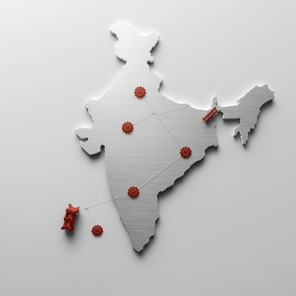
Building a genuinely independent semiconductor industry has become something close to a national obsession for governments worldwide over the past several years, and India’s own version of that ambition has just moved into a considerably more expansive second phase. The government formally notified the Semicon 2.0 scheme, setting in motion a Rs 1.27 lakh crore plan designed to deepen the country’s chip manufacturing and design ecosystem well beyond what its first phase managed to establish, opening participation to a considerably broader set of companies and institutions than the original programme ever covered.
The scheme’s structure reflects a deliberate attempt to address the semiconductor industry’s full value chain simultaneously rather than concentrating support narrowly on chip fabrication alone. According to the notification issued by the Ministry of Electronics and Information Technology, eligible applicants have been divided into six broad pillars spanning 10 distinct categories, extending from chip design startups and small and medium enterprises through to full scale semiconductor fabrication plants, assembly, testing and packaging facilities, specialised materials manufacturers, and even research organisations and training institutions focused on building the specialised talent pipeline the sector genuinely requires. That breadth stands in meaningful contrast to how the first phase of India’s semiconductor push was structured, which had approved 12 semiconductor projects across six states, with three facilities, Micron’s assembly, test and packaging plant, Kaynes Semicon and the CG Semi OSAT facility, having already commenced commercial production earlier this year.
IT Secretary S Krishnan framed the shift toward this second phase directly, stating that the time was now ripe to move toward developing a genuinely comprehensive semiconductor ecosystem through Semicon 2.0, with the scheme’s core objective centred on self reliance and fostering a globally competitive domestic industry. That framing matters because it signals a deliberate move away from treating semiconductor policy purely as an exercise in attracting large scale foreign fabrication investment, the primary emphasis of the first phase, toward building genuine indigenous capability across design, materials, equipment manufacturing and specialised talent, a considerably more ambitious and structurally difficult undertaking than simply courting a handful of large foreign fabrication plants to set up operations within Indian borders.
Reflecting on the evolution from the initial rollout, Union Minister for Electronics and Information Technology Ashwini Vaishnaw noted the changing global sentiment:
“When we started, there were genuine doubts about whether semiconductor manufacturing could really take off in India. Today, those doubts have been replaced by confidence.”— Ashwini Vaishnaw, Union Minister for Electronics and Information Technology
The specific eligibility and support terms laid out across different segments of the scheme reveal how carefully differentiated this second phase has been designed for the genuinely different economics that each part of the semiconductor value chain actually involves. For commercial chip design specifically, eligibility extends to Indian companies owned or controlled by Indian citizens or Overseas Citizens of India, including both startups and small and medium enterprises, with startups able to access financial support structured as grants and equity co-investment, while larger, more established companies can instead access royalty financing or equity co-investment depending on their specific circumstances. Silicon wafer fabrication, the considerably more capital intensive end of the value chain, carries a meaningfully higher bar for entry, applicants must propose a 300 millimetre wafer facility with a minimum capacity of 40,000 wafer starts per month, demonstrate possession of production grade licensed technology, commit a minimum investment of Rs 20,000 crore, and show minimum revenue of Rs 7,500 crore in at least one of the preceding three financial years, with the government providing 40 percent support toward eligible capital expenditure, a reduction from the 50 percent support level offered under the scheme’s first phase, reflecting either growing government confidence that the sector can now sustain itself with somewhat reduced subsidy levels, or a deliberate fiscal recalibration given the considerably larger number of categories this second phase now needs to support simultaneously.
Smaller scale segments of the value chain carry considerably more modest capital thresholds, reflecting the genuinely different investment scale each category realistically requires. Semiconductor grade raw material projects require a minimum capital expenditure of Rs 50 crore alongside Rs 20 crore in revenue, while dedicated test and characterisation facilities require Rs 100 crore in capital expenditure and Rs 40 crore in revenue respectively, thresholds set deliberately low enough to allow genuinely mid sized Indian companies, rather than only large conglomerates, to participate meaningfully in these specific segments. Equipment manufacturers supplying the broader chip production ecosystem will additionally receive production linked incentives ranging from 2 to 10 percent of the value of bills of materials sourced from domestic manufacturers, structured on a declining scale over five years beginning in the 2029 financial year, subject to an overall ceiling of 50 percent of eligible capital expenditure, an incentive structure specifically designed to encourage equipment makers to build genuinely domestic supply chains rather than simply assembling India based facilities around imported components.
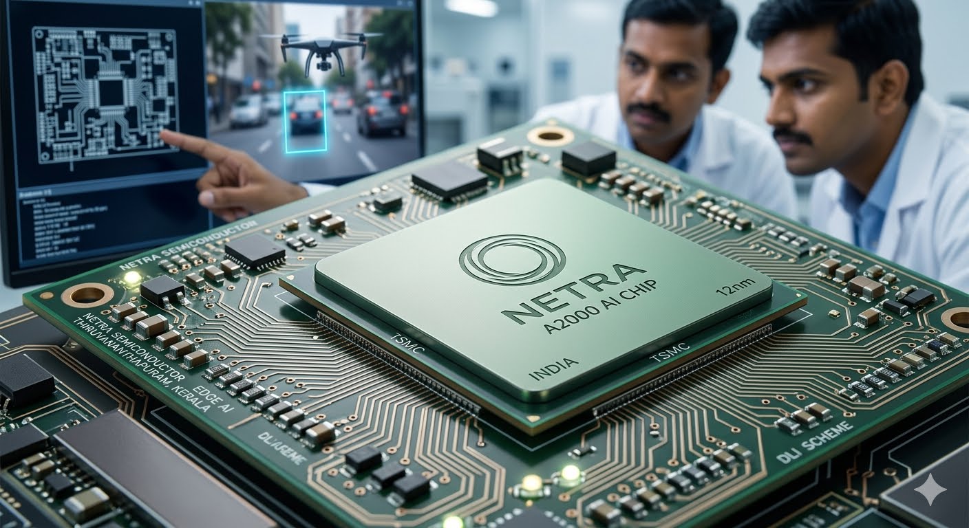
Chip design startups and small and medium enterprises specifically stand to benefit from a dedicated Design Infrastructure Support framework, granting access to national electronic design automation tools and multi project wafer fabrication services that would otherwise carry prohibitively high costs for smaller, earlier stage companies to access independently. These eligible startups and MSMEs can additionally seek seed funding of up to Rs 15 crore, capped at 50 percent of total project cost, while advanced semiconductor research and talent development projects can receive support covering up to 75 percent of project costs, subject to specific project conditions, an unusually generous support level that signals just how seriously the government has come to view talent and research capability as a genuine bottleneck constraining India’s broader semiconductor ambitions, separate from the more commonly discussed constraints around capital and manufacturing capacity.
Governance around which specific chip categories and products actually qualify for support under the scheme has been structured with a notably strategic, national security oriented framing. Ashwini Vaishnaw announced that a high level expert panel will be constituted specifically to identify which strategic semiconductor chips qualify for incentives, with that committee jointly chaired by the Principal Scientific Adviser and the National Security Adviser, a governance structure that places semiconductor policy decisions at a genuinely senior level of India’s national security and scientific policy apparatus rather than leaving those determinations purely to industry ministry officials. Detailing the broader strategic objective to build resilience and supply chain integration, Vaishnaw emphasized:
“People should feel dependent on India. People should become dependent on our country, on our industry, on our production, on our design.”— Ashwini Vaishnaw, Union Minister for Electronics and Information Technology
Vaishnaw indicated the panel will identify semiconductor products based specifically on their national importance and strategic priorities, and, when asked about areas where India could realistically achieve full domestic self sufficiency, pointed to sensors as a category where the scheme’s ambitions extend toward meeting up to 100 percent of domestic requirements through indigenous production.
It is worth situating this notification within the broader global context that has made semiconductor self reliance such an urgent policy priority across multiple governments simultaneously. Semiconductors have emerged as a genuinely critical strategic resource worldwide, with the artificial intelligence boom driving unprecedented demand for advanced chips and memory, while growing concerns over supply chain vulnerabilities and shifting geopolitical alignments have pushed governments and private companies alike to expand semiconductor manufacturing capacity and deliberately reduce dependence on any single concentrated source of supply, a dynamic that has made semiconductor policy considerably more geopolitically charged than it was even five years ago, when chip manufacturing was more commonly discussed purely in terms of industrial and economic policy rather than national security strategy.
Viewed evenly, Semicon 2.0 represents a genuinely substantial expansion in both the scale and structural sophistication of India’s semiconductor policy, moving deliberately beyond the narrower fabrication plant courtship that characterised its first phase toward a considerably more comprehensive attempt at building indigenous capability across chip design, materials, equipment manufacturing, testing and specialised talent development simultaneously. Whether this second, more ambitious phase actually succeeds in building the kind of genuinely self sufficient, globally competitive semiconductor ecosystem the scheme explicitly aims for will depend considerably less on the specific capital allocation figures announced this week and considerably more on execution discipline over the coming several years, converting notified eligibility criteria and announced financial support levels into genuinely operational fabrication plants, design houses and equipment manufacturers capable of competing on both cost and technical capability against considerably more established semiconductor ecosystems in Taiwan, South Korea, the United States and China that took decades, rather than a single funding cycle, to build their own current market positions.